Working principle of junction field effect transistor or jfet Diode formation depletion Miirbe pn junction diode reverse bias circuit diagram
To Draw The I-V Characteristic Curve of a P-N Junction In Forward Bias
P-n junction diode- definition, formation, characteristics Pn junction Semiconductor pn junction diode working
Solar cell working principle – studiousguy
P n junction diode,Diode junction bias pn reverse biased electrical4u diodes principle dioda voltage depletion kerja happens 1000v diyot nedir electron unbiased circuits Pn junction diode : i-v characteristicsDescribe briefly , with the help of a diagram, the role of the two.
Pn junctionJunction diode unbiased byjus diffusion conditions electron Junction reverse bias characteristic curve pn diode biased procedureKindly answer the question (a) draw v-l characteristics of a p-n.
Junction pn diode formation formed drift electrons
Semiconductor physicsWhat is a junction diode? what are the types of junction diodes Diode junction characteristics voltage elprocus theory working electrical its articleThe forward biased pn junction.
Forward and reverse bias of p n junctionDiode bias voltage biased across pn semiconductor applied varactor solar diodes circuits Diode junction operation cathodeTransistor field effect junction principle working electrical4u jfet november october.

Junction diode pn characteristics
Diode pn semiconductor junction layer bias reverse depletion working characteristics flow notes circuit current physics battery region biasing electronics typePn junction diode – formation, symbol, biasing, v-i characteristics P-n junction diode baising and its vi characteristicsPn junction anatomy.
Photodiode pn diode working junctionJunction pn electrical4u make between interface Explain pn junction with circuit diagramForward biasing of pn junction diode.

Formation of p-n junction diode || depletion layer formation || in
2.6 the p-n junctionFormation of depletion region in pn junction diode Diode junction schematic symbol pn forward biased type semiconductor silicon curve vs characteristic arrow technocrazed semiconductors corresponding electronics device advertisementExplain pn junction with circuit diagram.
What happens when a pn junction diode is forward biasedDiode junction pn bias forward characteristics depletion voltage electronics current region circuits mosfet connection formation biased reverse semiconductors under bjt Introduction to photodiode, pinout, working, features & applicationsForward junction pn biased potential barrier semiconductor height extremely led reduced physics.

Principle of pn junction diode
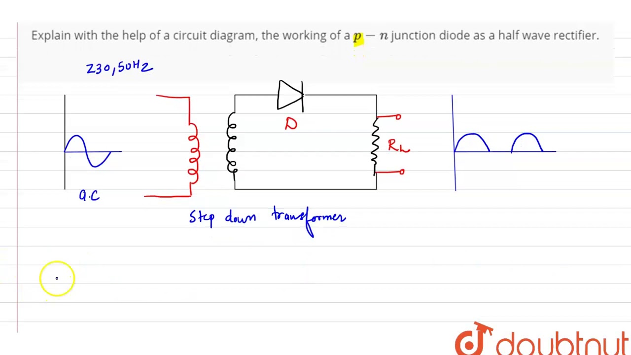
Explain pn junction with circuit diagramForward and reverse bias of a pn junction explained electrical4u Explain with the help of a circuit diagram, the working of a `p-nExplain how a potential barrier is developed in a p n junction diode..
To draw the i-v characteristic curve of a p-n junction in forward biasPn junction: what is it? (and how to make one) Diode operation.


Introduction to Photodiode, Pinout, Working, Features & Applications

What Happens When A Pn Junction Diode Is Forward Biased

Explain how a potential barrier is developed in a p n junction diode.

What is a Junction Diode? What are the types of junction diodes

semiconductor physics - Extremely forward biased pn junction - Physics

Describe briefly , with the help of a diagram, the role of the two

Formation Of Depletion Region In Pn Junction Diode - Riset